Browse categories
Explore
Fiverr Pro
English
$
USD
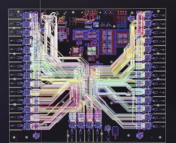
Professional PCB design engineer with 6+ years of experience. I offer full-cycle PCB layout, schematic design, reverse engineering, and manufacturing file generation.
Specialties:
Software: Altium Designer, Cadence Allegro/OrCAD, PADS, EasyEDA.
Deliverables: Complete schematic (PDF+source), PCB Gerber/Drill, BOM, Pick&Place files, 1 free revision.
Why me: 6 years of real-world experience, manufacturing-ready outputs optimized for JLCPCB/PCBWay, clear communication, on-time delivery.
Pricing: $1 per pad/pin for standard boards. Complex projects (DDR, impedance control, etc.) quoted separately.
Message me with your project details - I'll reply ASAP. Let's turn your idea into a working PCB!


| (0) | ||
| (0) | ||
| (0) | ||
| (0) | ||
| (1) |

esdi44

United States
Was not able to complete the assignment. I could not use any of his work. Would not recommend.
$50
Price
11 days
Duration
| (0) | ||
| (0) | ||
| (0) | ||
| (0) | ||
| (1) |
esdi44
United States
Was not able to complete the assignment. I could not use any of his work. Would not recommend.
$50
Price
11 days
Duration