Browse categories
Explore
Fiverr Pro
English
$
USD
United States
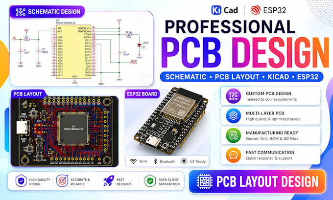
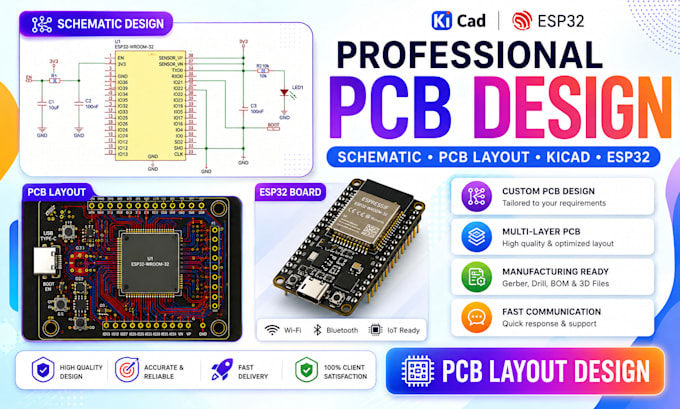
KiCad PCB Layout And Schematic Design for Arduino, ESP32 And Custom Circuits
Tired Of PCB Design That Fails At Fabrication? Many Buyers Get A PCB Layout Full Of Errors, Wrong Footprints, Or Gerber Files No Manufacturer Accepts, Wasting Weeks And Money On Failed Prototypes.
HELLO!
I solve that. I design clean, fabrication ready PCB layout in KiCad, EasyEDA, Altium or Eagle, from schematic design to finished circuit board. Whether it's an ESP32, Arduino, STM32, Raspberry Pi or any IoT smart device, your custom PCB design will be done right the first time.
WHAT YOU GET:
WHY BUYERS TRUST ME:
Clear communication, fast delivery, and full confidentiality on every hardware des ign project. I treat your electronics product like my own, no shortcuts, no guesswork.
Your Prototype Deserves A PCB Des igner Who Gets It Right.
MESSAGE ME BEFORE ORDERING, LET'S DISCUSS YOUR CIRCUIT AND START TODAY!
What if my board doesn't work after manufacturing?
If the issue comes from my layout, I'll fix it free of charge, no arguments. I stand behind every design I deliver.
I only have a hand-drawn sketch or an idea. Is that enough to start?
Yes! Many of my buyers start with just a rough sketch or a simple explanation. I'll turn it into a proper schematic and PCB layout step by step.
Can you keep my project private? I'm building a product to sell.
Absolutely. Your files, idea, and design stay 100% confidential. I never share, reuse, or showcase your project without your written permission.
Will you help me choose components that are actually in stock?
Yes. I check real-time stock on JLCPCB and other suppliers before finalizing your BOM, so you don't end up with parts you can't buy.
I'm not an engineer. Will I understand what you deliver?
Don't worry, I explain everything in plain English. You'll know exactly what each file is for and what to send to the manufacturer.