Browse categories
Explore
Fiverr Pro
English
$
USD
Expert Embedded Design Engineer, PCB Schematic and Design Specialist
Are you building an IoT product or a complex hardware system and need a professional PCB layout that is actually ready for manufacturing?
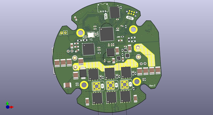
A poorly designed PCB can cost you thousands in manufacturing errors and delays. As an Embedded Design Engineer specializing in system architecture and IoT integration, I don't just route tracesI design for manufacturability (DFM) to ensure your prototype works on the first run.
My Expertise Includes:
Send me a message with your project requirements before placing an order so we can discuss the best architectural approach for your board!
File format:
Gerber
•
STEP
•
Software:
Altium Designer
•
EasyEDA
•
KiCad
•
Matlab
•
Proteus
Interface:
HDMI
•
I2S
•
UART
•
USB
•
SPI
•
I2C
•
Wi-Fi
•
BLE
•
GSM/GPRS
•
LTE
•
Ethernet
What software do you use for PCB design?
I utilize professional, industry-standard tools based on project needs, primarily focusing on Altium Designer, KiCad, and EasyEDA for precise multi-layer development.
What files will I receive at the end of the project?
Depending on the package, you will receive everything needed for manufacturing: Gerber files, NC Drill files, Bill of Materials (BOM), Pick & Place files, 3D Step files, and the original source files.
Do you do multi-layer PCB designs?
Yes, I specialize in routing up to 4-layer and 6-layer boards, strictly managing complex routing rules, ground planes, and signal integrity for advanced architectures.
Can you help if I only have an idea but no schematic?
Yes! Send me a message. I can assist with component selection, high-level system architecture, and drafting the initial schematic before we move into the PCB layout phase.