Browse categories
Explore
Fiverr Pro
English
$
USD
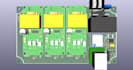
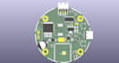
I design reliable, production-ready schematics and custom PCB layouts in KiCad tailored to your exact project specifications. From low-power microcontrollers to industrial power systems, I ensure your hardware is fully optimized for automated assembly.
What I can help you with:
Deliverables Included in Every Order:
️ Please message me before placing an order to discuss your circuit specifications, component availability, and delivery time.

Specialization:
Circuit design
•
Schematics
•
Layout
•
Footprint
•
Gerber
File format:
Gerber
•
STEP
•
SCH
•
Software:
KiCad
•
PSIM
I have a circuit design, can you convert it to PCB layout?
es, absolutely! If you already have a schematic (hand-drawn, image, or PDF), I can capture it in KiCad and design a production-ready PCB layout according to your dimensional and technical requirements.
What files do you need to design the PCB?
To get started, I will need your circuit schematic (or block diagram), dimensions/mounting constraints, component preferences (SMD or THT), and any specific connector placements or power requirements.
I have a project idea, can you create the schematic and PCB design for it?
Yes! If you only have a concept or functional requirements, I can help select the appropriate components, design the complete schematic, and layout the PCB in KiCad.
What specifications do you need to design the PCB?
I will need the board dimensions, enclosure constraints (if any), target input/output voltages, operating current, layer count preferences, and target manufacturer (e.g., JLCPCB, PCBWay).
What files will you provide me and what do I do with that?
You get KiCad source files, Gerber & Drill files for PCB manufacturing, and BOM & Pick-and-Place (CPL) files for automated SMT assembly. You also receive 3D STEP files. Simply upload the Gerber, BOM, and CPL files directly to vendors like JLCPCB or PCBWay to order your complete boards.
Can you help me sourcing the components and place the PCBA order?
I ensure all selected components are active and in stock (e.g., LCSC, Mouser) during design to avoid shortages. I will provide ready-to-use BOM and CPL files, but you will need to place the PCBA order directly with your manufacturer (like JLCPCB) using your own account.
Can you write the firmware for the project?
Yes! I can write embedded firmware for ESP32, STM32, Arduino, and Pi. Since firmware scope and features vary per project, please message me before ordering so we can discuss your exact logic, libraries, and custom requirements.
What gig package is suitable for my project?
The package depends on your circuit complexity, component count, and board layer requirements (2 to 8 layers). Please send me a quick message with your project details, and I will recommend the right package or send a custom offer!


