Browse categories
Explore
Fiverr Pro
English
$
USD
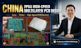
I am a China-based PCB Design Engineer with 10+ years of professional experience specializing in high-speed, high-density multilayer FPGA PCB design.
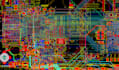
I have extensive experience with FPGA, BGA, DDR, SERDES, PCIe, USB, Ethernet, LVDS and high-speed ADC/DAC interfaces. My work goes beyond basic routing, focusing on the critical engineering factors that determine real-world reliability and performance.
I carefully address controlled impedance, stack-up design, differential pairs, length matching, signal integrity (SI), power integrity (PI), return paths, reference planes, crosstalk, EMI, BGA escape routing, high-density fanout, via structures, DDR timing, power distribution, thermal requirements and DFM.
A high-speed FPGA PCB is not simply about connecting nets. Signal integrity, timing, power, return currents and manufacturability must be engineered together.
I work professionally with Altium Designer and KiCad, delivering reliable, precise and manufacturing-ready PCB designs with complete production data when required.
Complex FPGA. High-speed signals. Dense multilayer design. Engineered for reliability.